| |
|
|
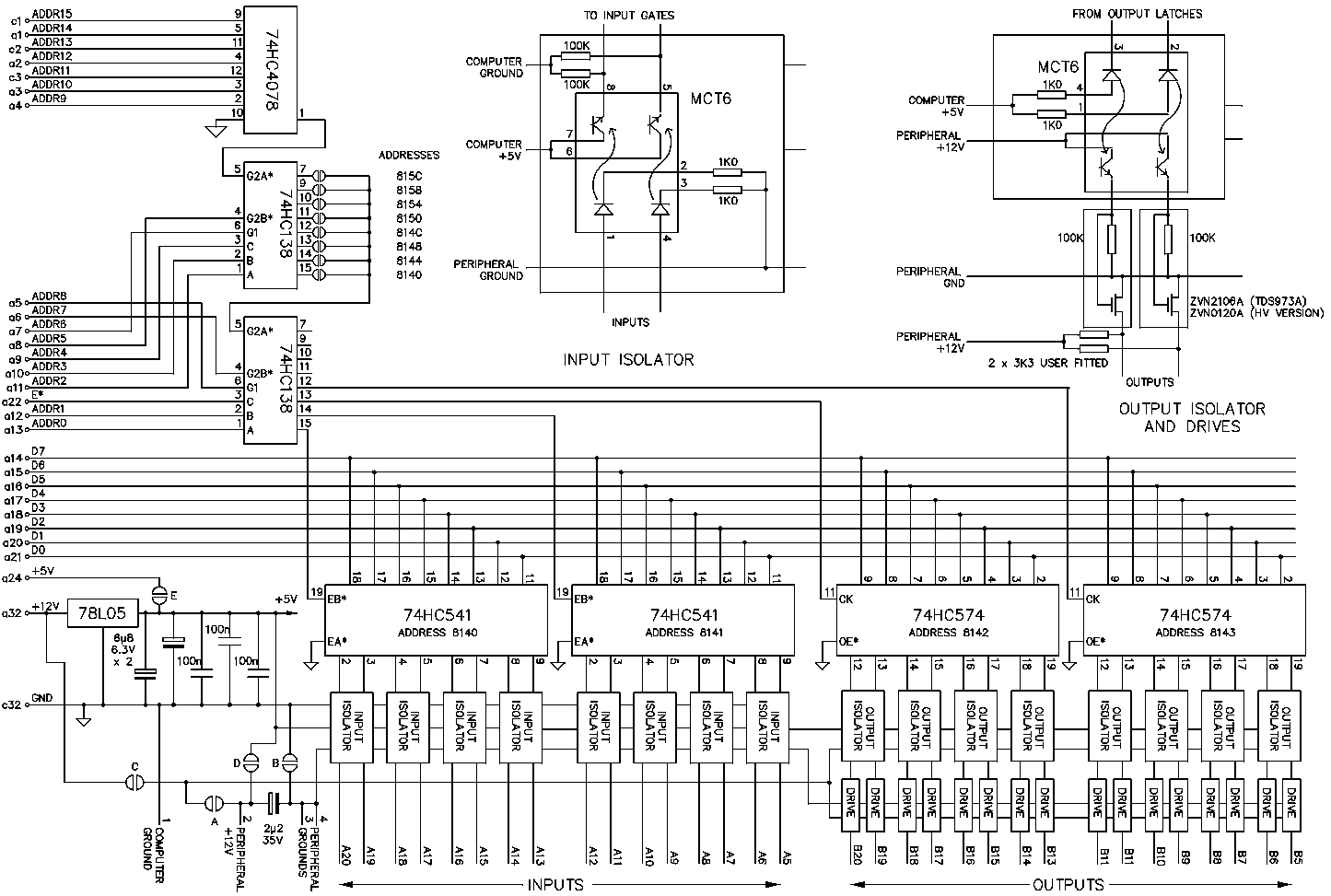
TDS973B PARALLEL I/O BOARDSThis product is obsolescent and should not be used for new designs with a long lifetime. The TDS973 is a general purpose input-output board for use with the TDS9092 computer (and other types). It provides an extra 16 parallel input and 16 parallel output bits. There are two versions, one is optically isolated, the other not. Up to eight TDS973 boards can be used giving a total of 128 inputs and 128 outputs. The format is single Eurocard (160 x 100mm) with 64-pin connector (you need TDS9092-PLUG type to work with this board). Pin connections correspond with the computer's. On the front are two 20-way shrouded headers for inputs and outputs. Inserted sockets can lie flush with the board edge provided the header latches are not fitted or removed. TDS973A16 inputs, 16 outputs optically isolated. The outputs of this version use power MOSFETs as switches with 60V/450mA capability. Typical ON resistance to peripheral ground is 1.0 ohm. Outputs are open drain (like open collector) but provision is made for user-fitting of pull-up resistors to the peripheral power supply. These are two single-in-line resistor packs and are put just behind the lower 20-way front connector, we supply two suitable 3K3 ohm packs with each board. The inputs are opto-diodes (inside the isolators) to ground and are in series with 1K0 resistors. This gives input logic levels of 0.0 to 1.0V (logic 0) and 4.8V to 30V (logic 1). A current of 8mA (at 12V) is drawn when logic 1 is applied. This means that input can be direct from micro- or reed switches since there is sufficient 'wiping' current to keep the contact clean. TDS973B16 inputs, 16 outputs without isolation. All CMOS. The outputs have logic levels of 0V (logic 0) and 5.0V (logic 1). Under load the outputs can source up to 4.0mA from 5.0V (giving logic level greater than 3.0V) and sink up to 8.0mA to ground (giving logic level less than 0.5V). The inputs are HCMOS gates needing logic levels of less than 1.3V (logic 0) and greater than 3.2V (logic 1) Other variations available to order include the following:
q Different front connectors. 20-way shrouded male types are standard. These have short latches for holding in the socket on a ribbon cable. We can fit vertical, unshrouded, female or non-latched connectors. q On the optically isolated version, MOSFET switches with 150V/160mA capability. These have a typical 8.0 ohm ON resistance and can be used for interfacing to higher voltage equipment. ADDRESSESThe address decoding from the Forth computer is done on the TDS973 Input/Output board and any board can be put at any of these hex addresses in the TDS9092 computer memory space:
0140 0144 0148 014C 0150 0154 0158 015C
In this way a system can have up to 8 TDS973 parallel I/O board giving 128 inputs and 128 outputs. Each TDS973 board is memory mapped to 4 bytes of computer address. For example, if a board is strapped to 0144 then the two input ports are addresses 0144 and 0145, while the two output ports are addresses 0146 and 0147. Note the full decoding for maximum use of address space. The addresses chosen are not used elsewhere on the TDS9092 for either memory or I/O. They are reserved for TDS973 use. On the TDS2020F the addresses are 8140 to 815C. SOFTWARESee the section PARALLEL INPUT & OUTPUT EXPANSION for examples of software interface to the peripheral ports. POWER SUPPLYOnly the +12V power supply on pin a32 is used since the TDS973 has its own on-board +5V regulator. If +12V is not available +5V can be used by supplying this on pin a24, making solder link E and removing the 78L05 device. Consumption of the TDS973B is about 1mA only since the board is constructed with CMOS devices. The TDS973A takes extra current of about 4mA per output channel at logic 0. For lowest power keep the outputs at logic 1 (open-drain) as far as possible. CONNECTORSOn the front of the board are two 20-way Insulation Displacement Connectors taking 20-pin low profile sockets on multi-way cable. Mating types include Electrospeed number 901-71240J. If ordering elsewhere make sure to request a '20-pin IDC socket for use with a plug with short-eared latches'. We can supply un-latched headers so that the socket will fit into the header and remain in line with the edge of the board. This enables the board to be used in a card-frame with flush front panel which also keeps in the connectors. All headers used except unshrouded types have built-in polarisation. This avoids wrongly connected ribbon cables. The rear connector is a DIN 41612 type C (two rows of 32 pins, 5.08mm apart). It can be connected directly across to a TDS9092 computer, via the TDS9099 backplane for instance. PIN CONNECTIONSREAR DIN 41612 CONNECTOR
UPPER FRONT CONNECTOR - INPUTS
** See the note at the end of the next section. LOWER FRONT CONNECTOR - OUTPUTS
** The +12V from the peripheral is used only on opto-isolated version TDS973A. It drives the output power MOSFET gates. Current consumption is 2mA maximum. If this is not available from the peripheral equipment use +5V for a slightly increased output impedance. If the peripheral has no power supply make links A, B and C in order to use the computer's +12V rail. The peripheral and computer grounds are now common however and some benefits of the opto-isolation are lost. On either board, making these links B and C can be useful in order to send the computer's +12V out to a peripheral with no supply of its own. If the +5V is preferred make links B and D.
TDS973 circuit diagram |
 |